a look inside the chips on the SX-70 camera (T.I.)
It has always been to take a look the dies of the electronics that run inside the SX-70. We were very lucky when the talented Ken Shirriff partnered with the project and helped us do just that. Hey wrote a blog post on his website that I highly recommend.
I am going to concentrate in the beautiful pictures taken by John McMaster
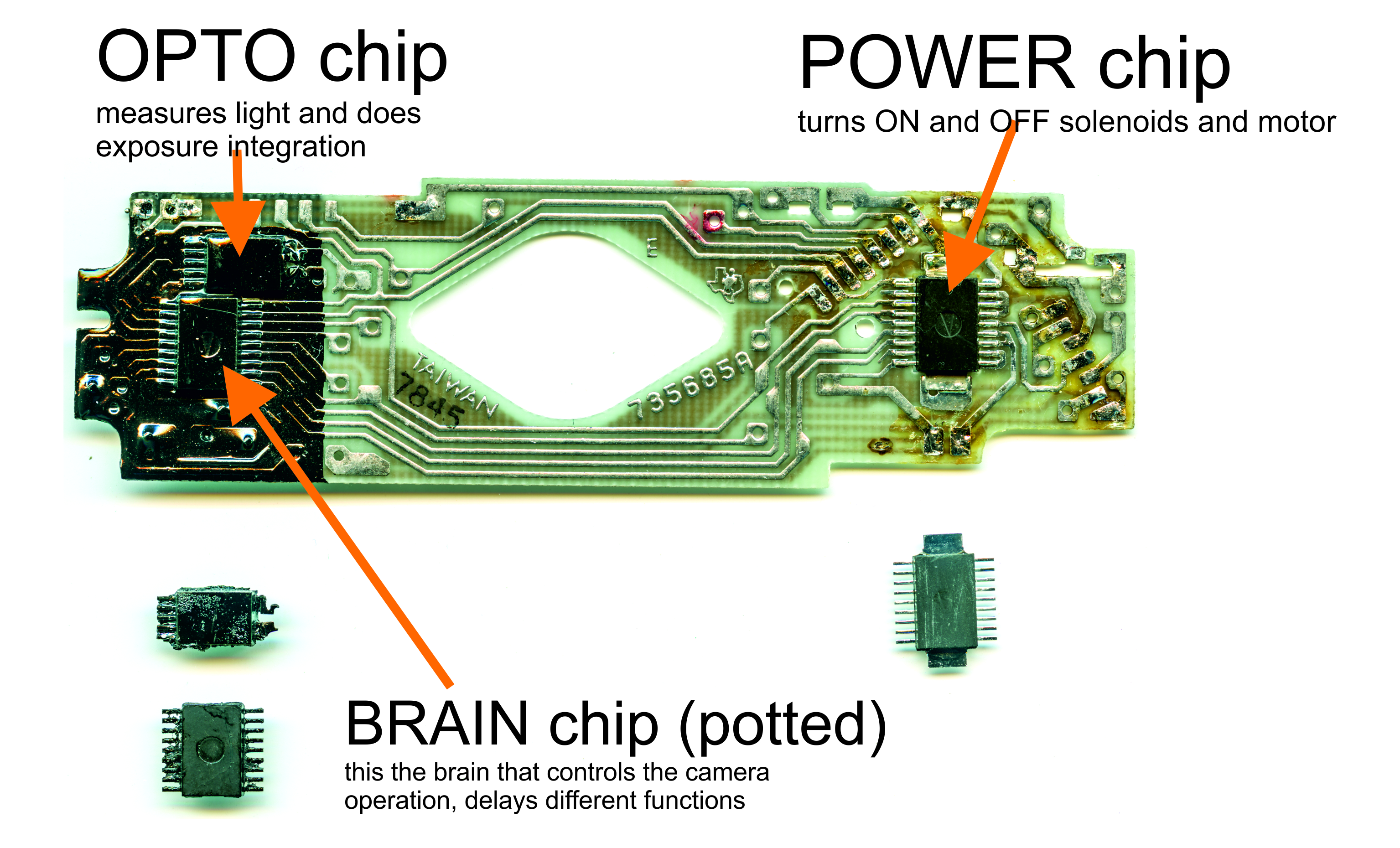
There are 3 chips in the main PCB of the SX-70 (ECM or Electronic Control Module in Polaroid lingo) the opto chip that controls the exposure called integration, the “brains” logic chip which is the one in control of all the cool stuff the SX-70 does, and finally the power chip, this is in charge of turning on and off the solenoids and the motor.
Please note that there were two companies that manufactured ECMs, TI (Texas Instruments) and Fairchild Camera.
If you want to know more about the competition between these company please read this post.
The optical chip
The camera exposed automatically the picture based on a system called integration, of course based on the ambient light. This is the source of the pictures.
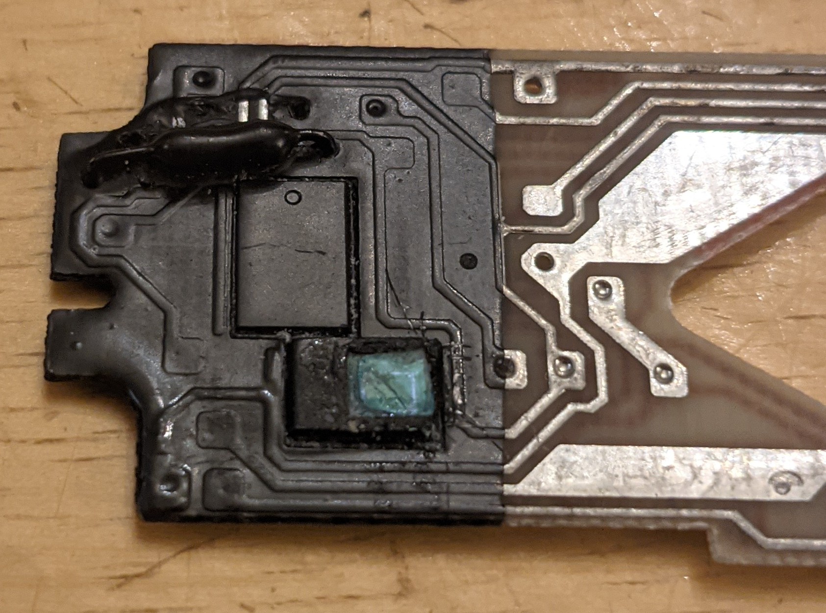


That is accomplished by the optical chip, this is not just a photodiode, but also contains a custom chip. That custom chip is a silicon die protected by epoxy, but the larger photodiode is exposed so external light can fall on it.

The optical chip contains a photodiode and a silicon die in one package.
.")
The optical chip. Photo from siliconPr0n, (CC BY 4.0).
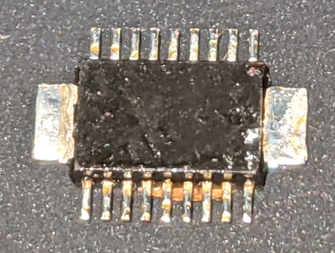
The “brain” logic chip
In Ken’s words:
The camera is controlled by a complex logic chip that controlled the timing of the various mechanisms, running the motor and solenoids. It had to handle four different use cases: ejecting the protective cover sheet when a film package was inserted, taking a photo, taking a photo with the flash, and ejecting an empty film package.n
This chip was constructed from Integrated Injection Logic (I2L), an obscure 1970s logic family featuring high density and low power. Because the camera ran off a battery in the film pack, minimizing power consumption was a critical factor. At the time, I2L was a good choice for dense, low-power circuitry, although it was soon overtaken by CMOS. Texas Instruments did a lot of development with I2L, including digital watch chips and the 76477 sound chip so it’s not surprising that they chose I2L for the camera chip.
.")
The logic chip. Photo from siliconPr0n, (CC BY 4.0).

Closeup of the logic chip.
![]()
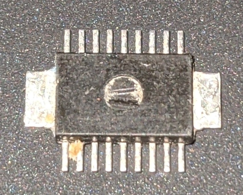
The power driver chip
Next, the power chip drives solenoids and the motor to activate the camera’s mechanisms. The high-current power transistors (the golden triangular shapes) take up most of this chip. Smaller transistors below form the control circuitry.
There is a vertical number 287121
.")
The power driver chip. Photo from siliconPr0n, (CC BY 4.0).
Conclusion
While the electronics of the SX-70 camera aren’t impressive by modern standards, they were cutting edge at the time. They made the SX-70 easy to operate by handling the exposure and timing automatically. Texas Instruments split the electronics across three chips: a precision JFET op-amp with a photodiode, a high-current power driver chip, and a complex logic chip using dense, low-power I2L logic.
Follow Ken on Twitter @kenshirriff for more posts. Thanks to John McMaster for decapping the chips.
Comments